

Technical Terminology
1.How to choose the right CL of crystals?
1) Recommended CL of crystals by IC
2) Empirical CL Calculation
CL≈C1*C2/(C1+C2)+Cs
(HC-49S Series: Cs=6pF; SMD Series: Cs=3pF)
C1, C2: Ground Capacitance of Crystal
3) Matching Experiment
Test the output frequency with different CL to find out the right CL for the circuit.
2. Frequency Tolerance
Max deviation value between operating frequency and nominal frequency at 25℃±3℃
3. Temperature Characteristics
Max deviation value between operating frequency and nominal frequency over operating temperature range
The frequency crystal resonator created is stable, but temperature has influence on it. The key determinant of temperature characteristics is angle of crystal cutting, the temperature characteristics curve shape is defined after crystal cutting. The temperature characteristics is described as below:
F=F0[1+a0(T-T0)+b0(T-T0)2+c0(T-T0)3]
T------- Random Temperature
T0----- Reference Temperature
F------- Frequency at T
F0 ------ Frequency at T0
a0, b0, c0------ Frequency-Temperature Coefficient at T0
Cubic curve of temperature characteristics------- When a0=0, b0=0 and c0≠0, widely use is AT cut
Temperature Characteristics Curve of AT Cut Crystal
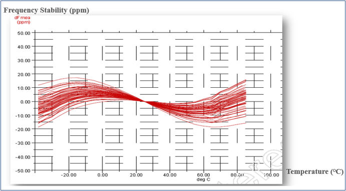
In mobile communication industry, temperature compensation is used to achieve the required stability due to the temperature characteristics of AT cut crystal is not good enough now.
4. Ts
Ts is a parameter describes the sensitivity for crystal to load capacitance, its definition is: the frequency variation of crystal when the load capacitance changes 1pF, unit is ppm/pF.
In normal frequency signal circuit, in order to guarantee the frequency stability of crystal in circuit, the smaller Ts, the better, because small Ts can reduce the impact on oscillating frequency caused by external circuit and environment.

5. DLD
DLD is the resistance variation when the drive level changes, and is also the dependency to drive level, everything on the crystal surface causes DLD rejects.

6. SPDB
Parasitism occurs because of the thickness difference of crystal, and the higher the frequency is, the greater parasitism will occur.

7. Negative Resistance
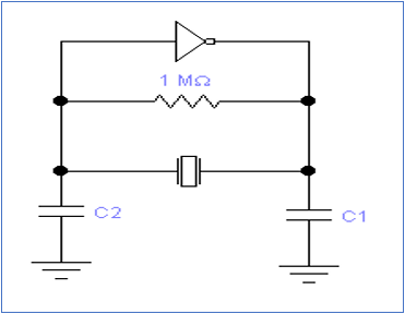
The Measurement Method of Negative Resistance

The connection diagram of Negative Resistance Measurement
1). Put the adjustable resistance and the crystal in series;
2). Increase the resistance (Rt) from 0 to the one lead to the oscillation of the loop get stopped;
3). Measure the Rt when the oscillation of the loop just get stopped;
4). The negative resistance is: │-R│= Rt+Rr
Rr: the resistance of the crystal;
Rt: the test value of the adjustable resistance
5). The recommended negative resistance is:
│-R│> 10 Rr (unit: ohm)
1. The resistance range of the crystal will be decided based on this measurement;
2. This measurement will also tell the vibromotive ability, oscillation amplitude, circuit stability, redundancy of resistance, and the suitability of the capacitances (C1, C2)
Remark: the capacitance of oscilloprobe which monitor the output amplitude of the oscillation circuit should be less than 1pF.
How to connect the adjustable resistance in practice?
1. Put the crystal upright, just leave one pad connected to the PCB (for SMD3225, it's the PAD of crystal connected to crystal blank, and the one near to the IC output port, not the GND PAD);
2. One end of the adjustable resistance connects to the other PAD of crystal (for SMD3225, it's the other PAD of crystal connected to crystal blank), the other end of the adjustable resistance connects to the PAD (the one was connected to the PAD of crystal) on the PCB, then the crystal and the adjustable resistance are in series.
3. The cable connected to the adjustable resistance should be as short as possible.
4. The carbon film resistor is recommended.